
Technologies
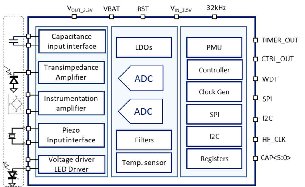
Sensor Analog Front-end IC
Features:
- Interface to raw sensor elements: Capacitance,
R-Bridge, Piezo, Current - 2-channel ADC with 16-bit resolution
- §Serial interface (SPI, I2C) to MCU
- Operates from 2 voltages, battery & 3.5V from
DC-DC - Built-in power cut-off feature to reduce standby current
- Test-chip in QFN88 package
Brief Specifications
| Physical parameters | Strain Temperature | Gas sensor (Optical) | Vibration | Pressure | |||
| Electrical interface | Resistance Bridge Voltage | Photodiodes LED | Piezoelectric sensor | Capacitance | |||
| Pre-amplifier | Instrumentation amplifier | Transimpedance amplifier | Charge amplifier | Capacitance-to-digital converter | |||
| Features | Low noise INA Gain: 200/2K/20K Input signal < 10kHz Range: 1μV – 10mV 3.3V, 3.5mA | Input signal ranges: 2 – 50nA & 0.5 – 50μA Single-ended inputs 1.8V, 4.5mA LED pulsed current drive: 3-100mA @3.3V | Pre-amp 50Hz – 10kHz < 1nF static cap | Direct digital converter 12-bit resolution SNR 72dB 10pF static cap (Test-chip), 500pF ES chip 1.8V, 200μA | |||
| 16-bit output ; 32 samples SPI readout in Test-chip / 1K in ES chip Programmable output 31.25KSPS / 15.625 KSPS ; 84dB SNDR 1.35mA, 1.8V | 5-bit oversampled output to be filtered externally | ||||||
| Digital &PMU | Serial interface SPI / I2C, Registers, Memory, Timers, CLK generator Programmable power management for the sensor node | ||||||
Wake-up RX IC
Brief Specifications
| Parameter | Value |
| Frequency range | 750 – 960MHz |
| Channel spacing | 200kHz |
| Data rates supported | Up to 50kbps |
| Power supply voltage | 1.2 – 1.5V |
| Avg. current consumption | 250μA |
| Peripherals | SPI |
| Operating temperature | -40°C to 85°C |
| Status | Test-chip |
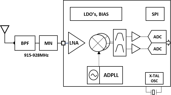
Application
- Command & control / Telemetry
- Pair with standard radio for battery life extension
Features
- The present design targets 900MHz band and IEEE 802.15.4g type radio. It can be extended with design modifications to other standards in 900MHz & 2.4GHz
- External band-selection filter (BPF) and impedance matching network (MN) are necessary.
- An MCU is necessary to build a complete wake-up radio function.
Energy Harvester IC
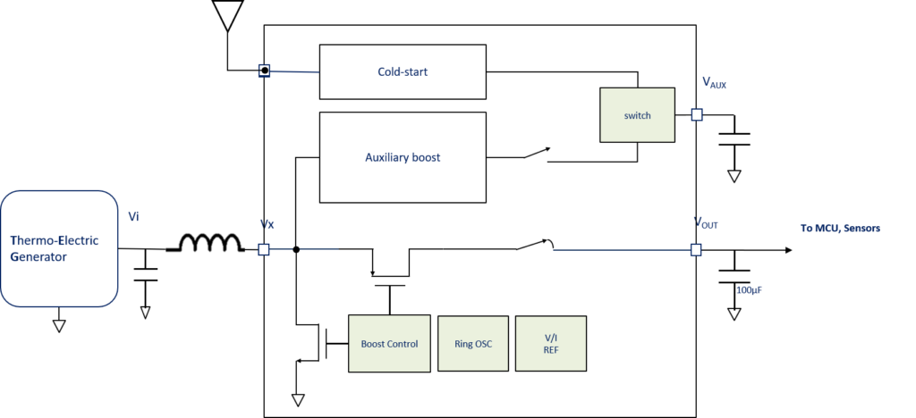
| Parameter | Value |
| Input voltage from TEG | > 25mV (after start-up) |
| Output voltage | 2.5V (regulated) |
| Energy storage cap | 100μF |
| Status | Silicon-proven test-chip |
Application
- Machine health/ infrastructure monitoring
- Wireless sensor nodes
Features
- Boost converter IC for energy harvesting.
- Powers MCU, Sensors, and low-power radio that are duty-cycled. For example, sense & store once every minute.
- Works with 25mV DC input voltage from TEG, after start-up.
- This design can be adapted for RF energy harvesting
- Novel cold-start mechanism
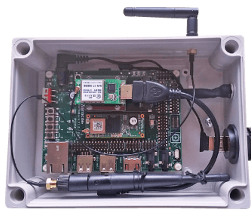
CME’s IoT platform

1. Sensor-Mate (sensing node)
- Long distance wireless communication (920MHz)
2. Sensor-Gateway (Aggregator)
- 920MHz wireless module (CM Engineering proprietary)
- Gateway includes control software for sensor data aggregation and system control
- Gateway supports internet and cloud server connection using TCP/IP protocol on Linux
3. Service system (configure & monitor)
| Frequency band | 920.6MHz – 928MHz |
| Data rate | 9.6kbps (50kbps/ 100kbps/200kbps supported) |
| Comms. distance | 1-2km (LOS) |
| # Sensor-Mate controlled by one Gateway | 200 (Sensor-Mate transfers data to Sensor-Gateway every 5 minutes) |
| Kind of sensors | Temperature, Humidity, Soil, Vibration, CO2, Voltage, etc. |